In this article we provide an introduction to near-eye optics, analyze the evolution of waveguides, then narrow the field down to holographic waveguides. Throughout we will examine the players in the waveguide OEM market (original equipment manufacturers), concluding with a focus on DigiLens of Sunnyvale.
What The Reader Will Gain
This article is not meant to be a scholarly treatise, but rather an accessible overview, providing the reader with a baseline understanding of the waveguide marketplace, and how advances in the field of optics are changing the landscape in the smartglasses market.
Near-eye Optics Basics
Most people remotely familiar with smartglasses have a general understanding of the display used in Google Glass, it is pretty basic: a micro-display (in this case a LCoS) is housed in the electronics attached to the side, and is pointed into a single prism that turns the light 90° into the upper-right-hand field-of-view of the wearer — in this case, a combined optical unit, housing both the LCoS display and the prism optics, supplied by HiMax (an optics OEM out of Taiwan).

Now imagine two of those 90° prisms set side by side. In this configuration one can turn an image 180°. Alternatively, two 90° prisms can also offset a display turning it back in the same direction. Shown here in its most simple form, this turning of the display is an important principle, as we move onto waveguides.

Waveguide Basics
Waveguides are not a new technology, per se. Waveguide displays are made using the same technology that allows a unidirectional wave of light to be guided down a fiber optic cable. When you look at a fiber optic cable from the side, you cannot see the light, only the dot of light at the end. Waveguide lenses use this same property of a unidirectional light-wave to guide a wave of light through a lens or plane (planar waveguide), from one end to the other.
Some of the most basic waveguides were first commercialized by Lumus Optics (coming out of Israeli military-industrial research). Lumus has more recently been the OEM supplier to both Daqri and Atheer.

Google and Sony both have intellectual property around waveguide designs similar in nature. A series of waveguide joint-research projects were also done by HiMax and Optivent of France; HiMax and Lumus; and Lumus and Essilor of France. Essilor is the world’s largest lens manufacturer, and recently merged with Luxottica of Italy, the world’s largest eye-frames company.
Surface relief waveguides
For a more sophisticated waveguide design, imagine a prism shrunk down to a very tiny scale, and elongated. Now engrave a series of these into the surface of a lens. These micro-ridges are referred to as a “surface relief” waveguide. The image is essentially sliced into a series of vertical stripes and reassembled by a corresponding set of micro-ridges on the other end of the lens, in front of the eye.

A surface relief waveguide of this kind was patented and first commercialized by Nokia.
The waveguides used in Microsoft’s HoloLens, are of Nokia’s design, modified with the housing turned upright, with the micro-displays placed above the eye.
Nokia’s patent is notable because it has shown to be mass-producible. Not only that, but in addition to HoloLens, Nokia has licensed this design to Vuzix, who manufactures their waveguides in a factory that was funded by an investment from Intel, and sold under co-brand with Lenovo on the Chinese enterprise market. This shows that Nokia’s design cannot only be mass-produced, but its manufacturing can also scale.
Others have been inspired by the surface relief design.
Dispelix of Finland has not only produced a surface relief waveguide, they’ve made a significant contribution to the manufacturing process. In addition to an engraved surface relief waveguide similar to Nokia’s (subtractive manufacturing), Dispelix has shown that a micro-ridge can also be created with an additive process, by “printing” the micro-ridges onto the lens.
Magic Leap

For a secretive company, we can learn a lot about Magic Leap from their patent filings and acquisitions, namely that they launched without a clear path to executing their vision.
Founder Rony Abovitz had previously taken public MAKO Surgical, a robotic arm surgical platform. MAKO then had a post-IPO acquisition by Stryker, the medical equipment giant (US $50B market cap), for a reported $1.65B. Given his prior unicorn exit, Abovitz had the trust of the investment community. Couple that with what we can safely assume was an impressive laboratory demo (in a controlled environment), and he was able to raise a staggering amount of money.
Magic Leap has experimented with a variety of optical designs in order to find a feasible light-field display that can be manufactured at massive scales. A light-field creates the effect of depth-of-field, allowing objects in focus to appear crisp and those not to appear blurry. For the kind of entertainment applications Magic Leap is pursuing, a light-field allows for a more realistic rendering of virtual content.
In April of last year Abovitz landed himself on the cover of Wired magazine with what was dubbed the Magic Leap “photonic chip.” The use of “chip” in the name referenced the manufacturing method needed to fabricate one of their theoretical displays.
Patents filed in 2013-2014 explore a variety of exotic optical designs, functional on paper, but with specifications outside the tolerances of existing manufacturing methods. The theory was that applying techniques used in the manufacturing of CPUs would make these displays possible. If one suspends all skepticism of Magic Leap’s potential success in such a manufacturing endeavor (and skepticism there is), they still faced two large obstacles, the first being cost: an eye-glass lens is several times larger in area than that of a modern CPU … and a pair of frames requires two of them. This means even if Magic Leap were successful in this approach, the lens fabrication cost alone would run into many thousands of dollars per pair, and they would lack the economies of scale enjoyed by companies like Intel who manufacture their chips in huge volume. The cost of glasses manufactured in this way would be extravagant. Secondly, buried within these patent filing are specifications suggesting lenses between one to one-and-a-half centimeters thick. Magic Leap is targeting the consumer market — even IF they could manufacture them, and even IF one disregards the manufacturing costs — not even the most remarkable displays would ever sell in a consumer market with a centimeter or thinker form factor. The devil is in the details.
At this point, it appears Magic Leap returned to the drawing board. The company’s patents also include a variation on a surface relief waveguide, stacked in layers. This brings us back to the aforementioned micro-ridge printing technique employed by Dispelix.
Last year Magic Leap quietly acquired a company called Molecular Imprints, whose proprietary technology is capable of printing micro-ridges, not dissimilar to Dispelix lenses.
This iteration of display could very well deliver Magic Leap a waveguide capable of producing a light-field display in a thin-ish form factor, for an affordable manufacturing cost. But with Dispelix already producing a printed surface relief waveguide, and with Avegant more recently demonstrating a light-field display (using an even more vintage beam-splitter technique), Magic Leap may have lost much of its novelty.
Holographic Waveguides
It would be easy to misinterpret the name. The “holograms” referenced in “holographic waveguides” do not refer to the image the wearer sees in front of them, but instead to the optics within the lenses, that are themselves made of nano-scale holograms.
Think of the hologram you see on a credit card. The hologram is exposed into a thin film that is adhered to a reflective backing (the reflective surface behind a credit card hologram is there to backlight it, the hologram itself is in front).
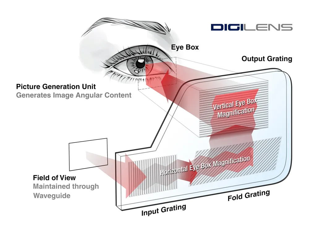
For holographic waveguides, a similar method is employed — a thin-film photopolymer is exposed with laser light to embed microscopic nano-scale holograms of mirror-like optics embedded within the lens, replacing the role of prisms in more traditional waveguides. Much as before, a micro-display is projected into one end of the lens, the hologram optics turn the light, guiding the unidirectional light-wave through the surface, and another set then turns the light back towards the eye. This remarkable feat of engineering is accomplished within a fraction of the thickness employed in prism-based waveguides.
DigiLens refined this technique almost a decade ago creating avionic HUD systems for the U.S. military (in collaboration with Rockwell Collins) that are still classified.
Holographic waveguide optics have seen several recent entries into their ranks: TruLife Optics and WaveOptics, both of the UK, and most recently Akonia Holographics of Colorado. Akonia had previously spent a decade, and burned through over $100M in an unsuccessful pursuit of holographic storage. These three companies appear to have now demonstrated in a lab environment, designs similar to what DigiLens was producing in 2010.

Since that time DigiLens has continued to innovate.
All of the previously mentioned waveguide designs are still “passive” lenses. Passive in that the lenses themselves have no electronic components, they simply receive the light projected by the micro-display, passively move the light through the lens, and turn it to project into the user’s eye.
Active Holographic Waveguides
DigiLens has “active” holographic waveguides.
Using a liquid crystal based thin-film polymer, the holographic mirror-like optics within DigiLens’ waveguides are able to change state when activated with an electric current.

Having started with military displays, DigiLens stayed in avionics and moved onto creating dash-mounted waveguide displays used in Embraer jets, again in collaboration with Rockwell Collins. Their first consumer product, a display for a BMW smart helmet, will ship later this year.
Furthermore, the aforementioned waveguides above are all constrained to a flat planar surface. Earlier this year DigiLens also announced they’ve perfected the application of their active holographic waveguides onto the surface of curved lenses, meaning they can apply them to regular prescription eyewear. They recently closed a $22M round co-led by Sony and Foxconn.
In a recent interview with DigiLens founder, chairman, CEO/CTO, Dr. Jonathan Waldern, he disclosed that they are also working on a laminate to apply to the inside of the lens, using similar technology employed in their waveguide display, but running off of a camera rather than a micro-display, to achieve eye-tracking in a similarly thin profile.
 This leaves only the optical novelty of a light-field outside of DigiLens’ existing offering. But if Magic Leap is achieving a light-field by using a multi-layered waveguide, DigiLens already employs multi-layered waveguides in their existing design — separating out the red color spectrum into its own waveguide, layered on top of a blue-green waveguide. Additionally, DigiLens has employed overlapping waveguides to expand the field-of-view. If they’ve not yet using their layered waveguides to achieve a light-field display it is because their client use-case has never required it — they have thus far specialized in contextual navigational data, rather than entertainment. If a paying client requested a light-field, it can safely be assumed they would build it to order, with their existing waveguide layering technology.
DigiLens is a sleeping unicorn. The success of smartglasses in a consumer acceptable form-factor begins-and-ends with near-eye optics, and Digilens might be at least seven years ahead of any other waveguide OEM in the game. While DigiLens’ work for the U.S. military may remain classified, it doesn’t take a breach of security to know that whatever Iron-Man HUD the U.S. military is building, it is DigiLens’ displays they’ve been using to build it.
Writer Christopher Grayson is an augmented reality, virtual reality and smart glasses expert market analyst represented by Gerson Lehrman Group. Grayson spent over a decade in the creative field of the New York City advertising industry, servicing technology accounts and premium brands, with award winning campaigns for Intel Vtune to the gaming industry, and Nikon professional digital SLR cameras to the fashion industry in collaboration with Emanuel Ungaro haute couture. In 2006, while working at Ogilvy, he launched the blog GigantiCo to discover what had come of VR and explore the emerging AR industry. As Executive Creative Director he helped launch Tokyo based smartglasses startup Telepathy. Grayson has been a speaker on augmented reality and smartglasses at SXSW, Microsoft Cambridge, New York Fashion Week, NASA Jet Propulsion Laboratory, and most recently at MIT Media Lab. Having recently relocated to San Francisco, he founded Reality Factory, a content focused VR collective, and will be hosting the Design Track at this year’s Augmented World Expo in Santa Clara.